最佳芯片验证工具
Cadence® Physical Verification System(PVS) 是由 EDA 软件商 Cadence 所提出之新一代芯片验证工具,它不仅能使用于类比 / 数字 / 混合信号之设计平台,如 Virtuoso IC Layout Platform、Encounter,且更与寄生参数萃取软件集成,如 QRC,以萃取布局后寄生参数,提供用户在芯片后段验证的完整解决方案。
随着半导体制程的发展趋势,芯片后段验证 (Back-end Verification) 所耗费的处理时间与复杂度不断提升的情况下,Cadence® Physical Verification System (PVS) 验证工具,凭其线性化的优异性能表现(Performance),不仅能减少运算处理时的等待时间;另外其创新的实时侦错 (Time-To-Error) 功能,实时侦错已运算完成部份,让使用者不再浪费时间等待运算结果,再者,其新创的人性化图形除错界面 (Graphic LVS Debug Interface ) 及交互式短路侦察系统 (Interactive Short Locator),不仅能有效弥补侦错经验不足的困扰,更能有效缩短来回除错所耗费的时间 (Turn Around Time),以提升工程师的效率及芯片产出。
此外,Cadence® Physical Verification System(PVS) 不仅同时支持 GDSII 与 Open-Access 的格式,亦兼容于目前工业界标准的验证语言,以降低工程师跨平台使用上的额外工作与难度。
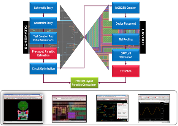
Physical Verification System (PVS) 流程图
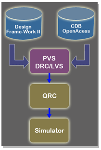
Physical Verification System (PVS) 后段验证解决方案

Physical Verification System (PVS) 特点
成功经验
 |
超过 50 位以上使用客户,包括晶圆厂及芯片设计公司 |
|---|---|
|
使用不同晶圆厂之不同制程下投片成功,包括成熟制程,如 130 / 90 / 65nm 及先进制程,如 45 / 40 / 28nm |
竞争力的性能表现
|
优异的单处理器 (singleCPU) 运算性能 |
|---|---|
|
支持单机多核心或多机多核心 |
|
线性化运算处理能力 |
有效率的分析及侦错接口
|
集成式侦错环境 |
|---|---|
|
实时侦错 (Time to Error) |
|
图形化除错接口 (Graphic LVS Debug Interface) |
|
交互式短路侦查系统 (Interactive ShortLoctor) |
跨平台集成
|
集成 Virtuoso customer IC layout platform 与 Cadence digital IC Encounter platform |
|---|---|
|
集成 Cadence QRC extraction,提升布局后寄生参数萃取之完整流程 |
晶圆厂级的设计服务
|
配合晶圆厂 Process Design Kits (PDK) 提供芯片设计所需文件数据 |
|---|---|
|
相容于台积电验证之 iDRC / iLVS design kits |
转换无障碍
|
相似之用户接口,熟悉度高易上手,操作无障碍 |
|---|---|
|
内建类似业界标准与法之 DRC / LVS 命令文檔,兼容性高 |
|
支持业界标准语法之 DRC / LVS 命令文文件 |
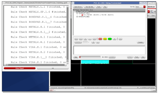
PVS DRC
|
Easy to use one window interface |
|---|---|
|
Time to error |
- Error Browser will pop up and allow viewing of errors while job is still running |
|
|
Standard DRC Browsing capabilities |
- By Cell/ By Rule |
|
|
Error Waivers |
- Persistent and loadable in subsequent runs |
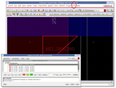
Time To Error
Error Browser will pop up and allow viewing of errors while job is still running.
PVS LVS
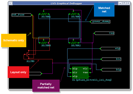
Rapidly identifies complex LVS mismatches
|
Graphic LVS Debug accelerates identification of complex LVS mismatches in chip designs |
|---|---|
- Compares logical and physical design using a common schematic representation |
|
- Guides navigation using design errors |
|
- Can be launched with LVS debug environment, and graphical elements can be probed through the LVS debug environment |
|
- All errors and warnings are easily navigated and show surrounding context |
Strong functionalities and flexible usability
|
Error Tags |
|---|---|
|
World view or detail view |
|
Filter net, devices for better understanding of error |
|
Drill down for more information on points of interest |
|
etc |
LVS Hyper debugger - Graphical LVS Debug
LVS debug is extremely time-consuming and experience dependent
|
Limitation of current tools |
|---|---|
- Static error report in batch mode, contain large data, difficult to understand |
|
- Errors in text report hard to identify relationship |
|
- User cannot actively query more information on points of interest |
|
- Not allow easy navigation of the original design |
|
|
Bind-key - Cadence Composor like |
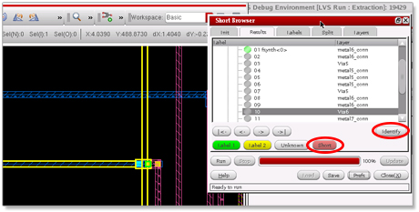
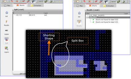
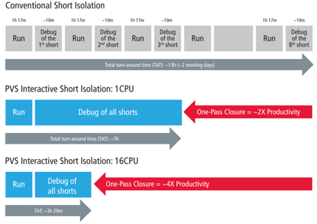
One-pass short isolation
|
Locating shorts found in old-fashion LVS comparison report requires |
|---|---|
- Additional manual work |
|
- Additional LVS extraction and comparison runs |
|
|
PVS approach facilitates one-pass short isolation for cell / block / full-chip designs |
- Run time typically <10% of extraction time and scales up to 5x with 8 CPUs |
|
- Start debugging while run is in progress as soon as first results are available |
Interactive Short Locator - Comparison with and without the Interactive Short Locator
PVS to QRC interface
Fully solution for back-end verification
Support Cadence QRC flow to complete post-layout simulation
|
No additional licenses required to enable flow |
|---|---|
|
Provides complete QRC GUI support |
|
TECHLIB feature makes PVS QRC flow easy to use |
|
Batch / interactive use model |
|
Support Spice, SPEF, DSPF, extracted view, etc. flows |
|
Parity of flow between PVS / Assura = easy transition |